
EEV44-82 CCDs Performance overview
Best viewed with 1024x768 resolution
Oct/10/1999, C. Cavadore
Generality
The company EEV supplied ESO with many custom designed CCD called EEV44-82.This CCD has been used in many systems at ESO, such as WFI, VLTTC2, UVES,VIMOS, CES …
This device has 2 readout ports. The CCD can be operated either in dualreadout mode using two ports, or single port readout. Binning along theX and Y direction is possible using any kind of binning factor providedthat the scene is not oversatured. A fast wiping of the device can be achievedby using a dump gate close to the serial register.
This table summarizes main CCD geometrical dimension.
| EEV 44-82 | Full Frame / Frame transfer capable | |
| Type : Backside, Single layer AR | Pixel size 15x15 mm100% photosensitive | |
| Number of photosensitive pixels | 2048 x 4102 [HxV] | Number of outputs : 2 |
| Size of the photosensitive area | 30.72 x 61.53 mm | |
| Horizontal pre-scan pixels | 50 | |
This device is 3 sides buttable. For each device, the theoretical nonsensitivity side area is 100 microns and the Left-Right gaps are 450 micronseach.
Noise
The following table shows noise performances achieved with FIERA atdifferent readout speeds and conversion factors (e-/ADU).
(kps) |
(e-/ADU) |
(e- rms) |
|
These noise figures may vary slightly according to the device used.
Quantum efficiency
EEV has optimized the QE to get good QE in the B and U bands. Nevertheless,depending on the device, the QE in this range may vary slightly. The explanationis the following: the Quantum Efficiency of these devices is strongly relatedto of the thickness backside Anti-Reflection coating and this thicknessmay vary according to the device (Hafnium Oxide 50nm). ESO measured 12devices and used to achieve a statistic QE plot (figure A). Thisis a criterion also to sort science grade devices : the best QE in theblue (except for application requiring a higher red sensitivity).
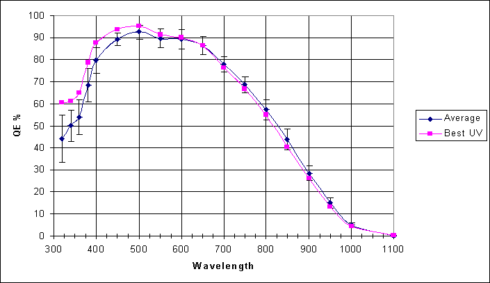
figure A: Average QE of 12 devices, error bars shows the QE standarddeviation from these 12 devices. Also the best blue sensitive device isplotted.
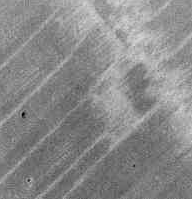
Fringing
Fringing is an issue for spectroscopic purposes. ODT has measured thiseffect with 8 devices. The resulting parameter is called PRNU across thechip (Photo-response non-uniformity). The near IR PRNU depends upon thefringing effect. This effect is related to the thinning of the CCD, andalso to the aperture of the incoming beam, the more this beam is open,the less the fringing is visible (figure B). In the blue part ofthe spectrum the PRNU degrades also due to the backside p+ implementationlaser annealing. The images (figure C) show qualitatively theseeffects. Figure C is a statistical analysis over 8 CCDs.
 320nm
320nm 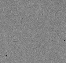 650nm
650nm 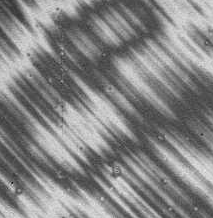 950nm
950nm
figure B : Flat fields from the same area at different wavelengths,5nm bandwidth, parallel incoming beam, left 320nm, middle 650nm, right950nm, F/2 beam.
300x300 pixels POSITIVE IMAGES
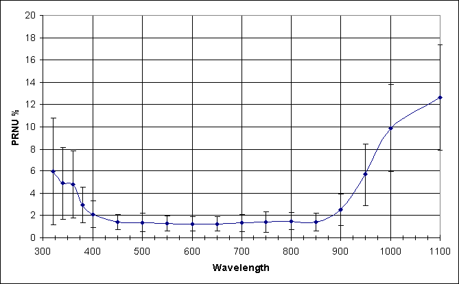
figure C: Average PRNU form 8 devices, error bars shows the PRNUstandard deviation from these 8 devices, F/2 beam.
Cosmetic defects
The different kind of defects, which degrade the cosmetic quality ofthe device, can be split in three parts :
- Defects visible in the bias images (mainly hot pixels)
- Defect visible with a low light level flat field (traps, figure F)
- Defects visible in the median stack of 5 1h exposed dark frame (mainlyoversatured hot pixels, trails, figure D,E)
A defect is a pixel value above or below 5 sigmas from the meanof the neighborhood pixels.
These defects are based upon the grading of the device, typically agood science grade is one with less than 5 defective columns. The amountof defects visible on long dark exposure is strongly related to the CCDtemperature. An operating CCD temperature of –120C is used to minimizethese effects.
Also the CCD device is made of 1024x512 blocks, and the area boundariesshow sometime a 1% QE variation over 1 row/column due to photolithographystepper mismatches. These small defects flat-field out perfectly.
Trap defects are a determining factor for assigning devices to certainapplications. These kind of defects cannot be suppressed because they arecreated during chip fabrication, and are not temperature dependant.
Finally, the amount of the "defects" induced by cosmic rays should notbe more than the one provided by natural radioactivity. The CCD packageand the head of the detector do not add additional hits. This value istypically between 1 and 1.5 event/min/cm2.
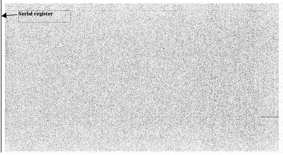
Figure D, Median stacked of 1 hour exposure dark full frame of ascience grade device (CCD A for spectroscopy) at –120C, only 3 hot columnsare visible (overview of the entire device)
NEGATIVE IMAGE.
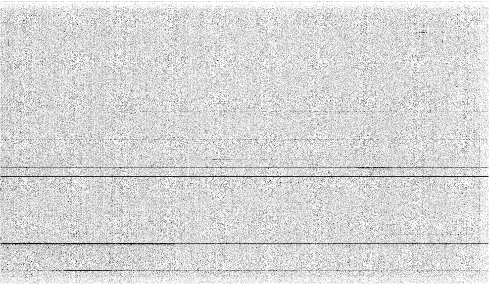
Figure E, Median stacked of 1 hour exposure dark frame of a mediumgrade device (CCD B for direct imaging) at –120C, 8 hot columns are visible(overview of the entire device)
NEGATIVE IMAGE.
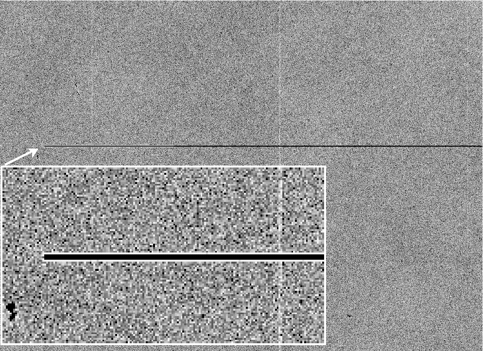
Figure F, Low light level frame (2000e-): a 5 column wide trap isvisible here (overview of 1300x900 pixels). This device is rejected forspectroscopic applications.
POSITIVE IMAGE
Charge transfer efficiency
ESO measurements shows horizontal CTE of 0.9999995 (six 9s, 5) and verticalCTE of 0.9999988 (almost six 9s). It means in the worst case : A pixelhaving 1000 electrons located on the opposite side to the readout port(X=2048, Y=4100) will lose 6 electrons, once the charge packet will reachthe readout node (photon shot noise is about 31e- at that level).
Dark Current
EEV44-82 devices do not have MPP implant. The dark current is temperaturedependent as shown in figure G. The CCD must be cooled at a temperatureless than –95C for science purposes to achieve a dark current less andequal to 10 e-/pixel/hour :
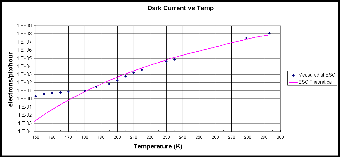
Figure G: Dark current versus temperature
(e-/pix/hour) |
|
Amplifier glowing
To avoid amplifier glowing, voltages less than 25 volts must be setto the VOD node of the chip.
Remanence effects
Remanence effects may occur if a flat field (Mean>10000e-) is takenprior to the dark frame. The resulting effect resembles an increase ofdark current, especially at temperatures lower than 180K. ODT is currentlyinvestigating to cure this problem. Figure H, shows a set of 24 dark framesexposed each one-hour (CCD temperature : 160K). This set was taken afterthe CCD was exposed to the ambient light. It requires four 1 hour darksframes to eliminate of the remanence and to reach the actual dark currentvalue (about 5e-/pix/hour).
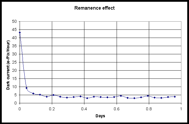
figure H: Remanence effect

figure Ha : oversaturated spot,
negative image

figure Hb : one hour dark exposure, just after Ha figure, binned10x10, plus cosmic hits,
negative image

figure Hc : one hour dark exposure, just after Hb figure, binned10x10, only the central spot is visible, negative image
Bright Star/bright spots remanent might be also visible when doing longexposure afterward. Figure Ha shows an oversaturated star, withintense vertical blooming. Figure Hb shows one hour dark exposuretaken just after at –120C. The blooming and central spot ghost are stillvisible. If additional images are taken, it disappears after 4 hours. From that study, It means that remanance has a global and local effects.
| T+1h | T+2h | T+3h | |
| Central Bulb remanent (e-) | 8 | 6 | 2 |
| Blooming remanent (e-) | 2 | 1 | 0 |
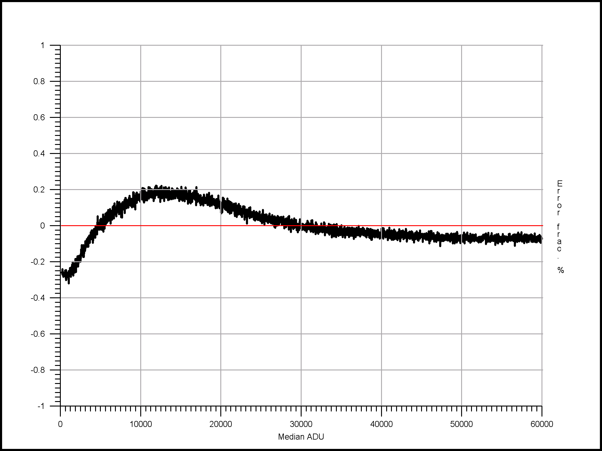
Linearity
By optimizing the voltages applied to the CCD readout amplifier, a goodlinearity can be achieved in the range of 0-100Ke- without degradingnoise performance. The table below summarizes a typical linearity performancefrom an EEV device at 225Kps.
(e-) |
|||||
| Port A (left bottom) | |||||
| Port B (right bottom) | |||||
| Left and Right Port (225kps) | |||||
 |
|||||
Best performance is achieved with p-p linearity of ?0.35%. Special voltage optimization is performed to get ?0.5% at least across the full range.
Flatness
ODT has developed a special measurement device to acquire full chipsurface profile. A typical value is typically ?6 microns at 150K, a maximum value is ? 10 micronsp-p.
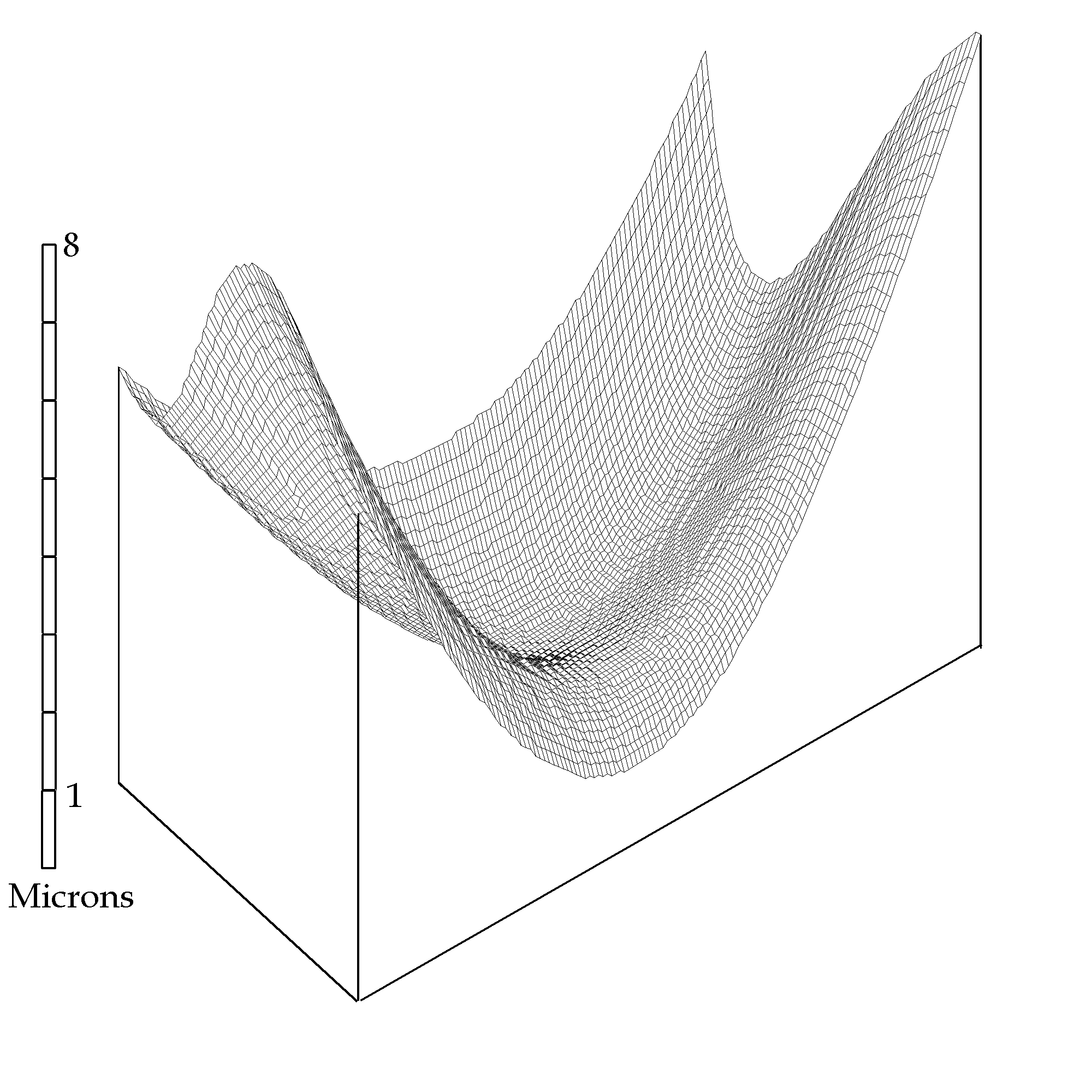
figure I : Typical 3D plot of the CCD surface
MTF
According to ODT’s latest measurements, the CCD shows no serious degradationfrom the Nyquist curve. The very sharp hits resulting from the cosmic rayimpacts show that 95% of the energy released is within one pixel.
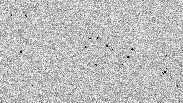

figure J : Cosmic rays hits (1 hour exposure), enlargement showing4 cosmic rays hits
NEGATIVE IMAGE.
Binning eclipse effect on saturated stars
When using binning more than 1x1, a saturated star appears with a strangeblack hole in the middle. The CCD output amplifier is, in this particularstate, completely out of range and behaves strangely. As there is, anyway,no useful information in the center of a saturated star (no photometry/astrometryfeasible), this effect is more a cosmetic issue (which could be eliminatedby software) than scientific.
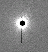
figure K : Eclipse effect on a saturated star with binning 2x2
POSITIVE IMAGE.
Blooming effect
To avoid loss of fill-factor, this CCD has not antiblooming implant.This causes vertical trails over bright and saturated stars. The tablebelow gives a crude indication of the order of magnitude for point sources.L1 denotes the number of pixels concerned toward the serial register, L2the one in the opposite direction. Measurements made with binning 1x1.
| Direction | ||||||||
| L1(pixels) | ||||||||
| L2(pixels) | ||||||||
Cross talk effect
This CCD allowing two port readout in the same time could exhibit crosstalk between two channels. It could be visible when a bright star is presentover the CCD. This effect has been measured at ESO. If an over saturatedbright spot is projected over one side of the CCD, ghost having an additionalfix level of 100 e- is visible on the other side, with the same shape ofthe original bright spot. This is, for all imaging purposes, a negligibleeffect.
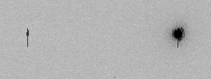
figure L : Cross ta with a saturated star and 2 port readout
NEGATIVE IMAGE.