
SofI Detector Characteristics
Hawaii Detector
SOFI is equipped with a 1024x1024 Hawaii HgCdTe manufactured by Rockwell Scientific. Bellow is a table with short description of the array properties. The information on this page is taken from the web site of the array manufacturer.
Array Characteristics
| Array Format | Hawaii HgCdTe 1024x1024 |
| Pixel Size | 18.5 µ |
| Q.E. | ~ 60% |
| Gain | ~ 5.4 e/ADU |
| RON | ~ 2.1 ADU |
| Bad Pixels | About 10000 |
| Non-Linearity | < 1.5% over 0 to 10000 ADU |
| Dark Current | < 0.1 e/s |
Quantum Efficiency
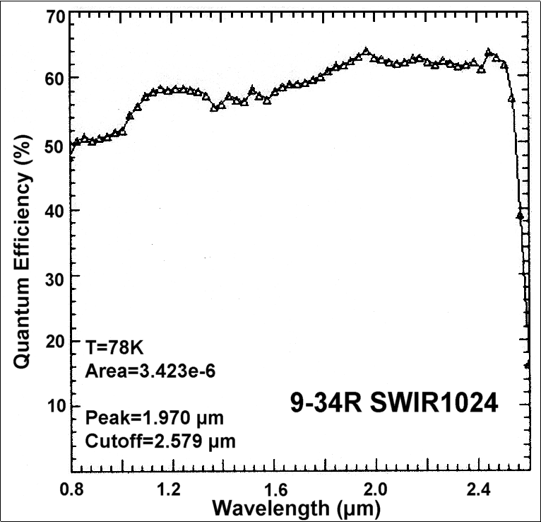
An ASCII table with the detector Quantum Efficiency curve is available.
Readout Modes
The HAWAII 1024 x 1024 readout is structured in four independent quadrants having four outputs. Six CMOS-level clocks, two 5V power supplies (one analog and one digital), on e fixed dc bias and one variable dc bias are required for basic operation. The multiplexer architecture has been optimized to minimize glow. The goal of < 0.1 e-/s has been achieved using correlated double sampling. Read noise of < 10 e- has also been achieved due to refinements in the readout design to suppress the pixel reset anomaly associated with earlier astronomy arrays such as NICMOS3.
Each quadrant contains two digital shift registers for addressing pixels in the array; a horizontal register and a vertical register. Each register requires two clocks; one dual edge triggered clock and one level triggered clock. To obtain a raster scan output, the horizontal register is usually clocked in the fast direction with the vertical register being clocked in the slow direction.
Horizontal Register
Pixel and Lsync are the two required clocks for the horizontal register. The Pixel input clock is a dual edge triggered clock which will increment the selected column on both edges (odd columns selected on positive edges and even columns selected on negative edges). The Lsync clock is an active low input which will set a '0' in the first latch and a '1' in the remaining latches of the shift register, thereby initializing the shift register to select the first column in the quadrant. Since this is asynchronous to Pixel clock, Lsync should be pulsed low prior to initiation of the first Pixel clock edge. The horizontal register selects which column bus will be connected to the output source follower amplifier.
Vertical Register
Line and Fsync are the two required clocks for the vertical register. The Line input clock is a dual edge triggered clock which will increment the row selected on both edges (odd rows selected on positive edges and even rows on negative edges). The Fsync clock is an active low input clock which will set a '0' in the first latch and a '1' in the remaining latches of the shift register, thereby initializing the shift register to select the first row in the quadrant. since this is asynchronous to the Line clock, Fsync should be pulsed low prior to initiation of the first Line clock edge. The vertical register selects the row to be read and/or reset depending on the ResetB and Read inputs.
ResetB and Read
The two remaining clocks are ResetB and Read. These two clocks are used to gate with the vertical register outputs to form the line reset and read function of the multiplexer. ResetB is an active low clock which will reset all of the detectors in the selected row to the voltage Vrst (supplied externally off chip). Usually the process of resetting the detector array involves addressing the desired row to reset using the vertical shift register, and pulsing the ResetB line low. The Read clock is an active high clock which will allow signals from the currently row to be transferred to the column (vertical) buses. The column buses are input to horizontal register controlled transmission gates. The output of the transmission gates is the horizontal bus, which is input to the output source follower amplifier. The horizontal bus can also be directly accessed through the Bus pins on the chip carrier.
Correlated Double Sampling (CDS)
CDS is a clocking method by which the array is reset, sampled, allowed to integrate, and re-sampled with the difference between the 1st and 2nd samples being recorded. CDS is effective at reducing noise and eliminating detector offsets.
For long integration times, IR glow from the output source follower amplifiers will be evident in the image as high dark current areas in the corners of the array. The glow will be on the order of 1,000's of electrons/sec but can be reduced by minimizing the output source follower conduction during integration.
Turning off the source follower amplifiers can be accomplished by ensuring that the gate of the PFET output source follower is pulled high (+5V) when not in use. This occurs when the Read input clock is pulled low, hence disconnecting all of the column buses from the gate of the source follower. The gate will be pulled up via the Biaspwr bias input.
Biases
Only 2 of the 14 biases, Vrst and Biasgate, will require voltage adjustment during operation of the hybrid. Vrst is the reset voltage that gets applied to the detectors during the reset operation. This voltage is applied through an NFET reset switch which has an associated voltage drop across it due to parasitics of the reset FET; hence, this will reduce the actual voltage to the detector by about 100mV - 150mV. Vrst is usually operated in the 0.5V to 1.0V range.
Biasgate is used to adjust the speed and dynamic range of the unit cell source follower. A trade off can be made between speed and dynamic range by adjusting Biasgate from 3.3V to 3.8V. Lower voltages increase the speed at the expense of dynamic range, while higher voltages increase the dynamic range at the expense of speed. A typical Biasgate voltage of 3.5V is used for initial characterization of the hybrid.
Source and Bus Outputs
The Source and Bus pins on the carrier are two simultaneous outputs available on the multiplexer. Source is connected to the source of the output source follower; by using a pullup resistor of 10Kohms to +5V, the multiplexer can directly drive off-chip loads such as cables and preamp inputs. Bus is connected to the gate of the output source follower. A 200Kohms to +5V pullup resistor is required if the user would like to use this output and provide their own off-chip driver.
NICMOS3 Functional Comparison
For those who are familiar with Rockwell's NICMOS3 256 x 256 SWIR focal plane array, the transition to the HAWAII 1024 x 1024 SWIR focal plane array should be relatively easy; however, there have been some slight changes to the basic architecture which should be noted:
- Replacement of the pixel reset with a line reset.
- Replacement of the Clear clock function with a Read clock function.
- Reduction of pixel pitch from 40mm to 18.5mm.
In an attempt to reduce the effects of noise caused by resetting pixels in the array (reset anomaly), the HAWAII multiplexer has a line by line reset instead of a pixel by pixel reset. This means that at any time while accessing a row, the entire row will be reset when ResetB clock is pulsed low. In order to reset an entire frame using NICMOS3 it is necessary to address every pixel in a quadrant, however, in order to reset an entire frame using the HAWAII multiplexer it is necessary only to clock through the vertical register.
Both NICMOS3 and HAWAII require 6 input clocks to properly operate the array. Both require 2 clocks per shift register; however, for HAWAII, Lsync should be pulsed low before the first Pixel clock edge for the horizontal register and not during as is the case for NICMOS3. This also true for Fsync and Line inputs for the vertical register. The Line clock for HAWAII is dual edge triggered, not negative edge triggered as in NICMOS3.
The two remaining clock inputs are ResetB and Read. While accessing any row in the array, pulling the ResetB input low will simultaneously reset all pixels in that row; this is in contrast to NICMOS3 which requires the accessing of every pixel which is to be reset. By pulling the Read input high, the currently selected unit cell source follower is allowed to pass to the column bus. This also means that anytime the Read clock is low, none of the unit cell signals can be transferred to the output source follower via the column buses; regardless of the state of the horizontal or vertical register. This feature is very useful in turning 'off' the output source follower when not in use to decrease the effects of the output source follower glow. NICMOS3 required an extra horizontal register Pixel clock at the end of the row in order to ensure that the output source follower was 'off'.
Gallery
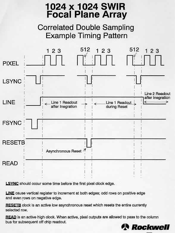 |
Correlated double sampling readout mode |
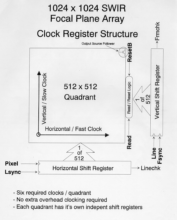 |
Clock register structure |
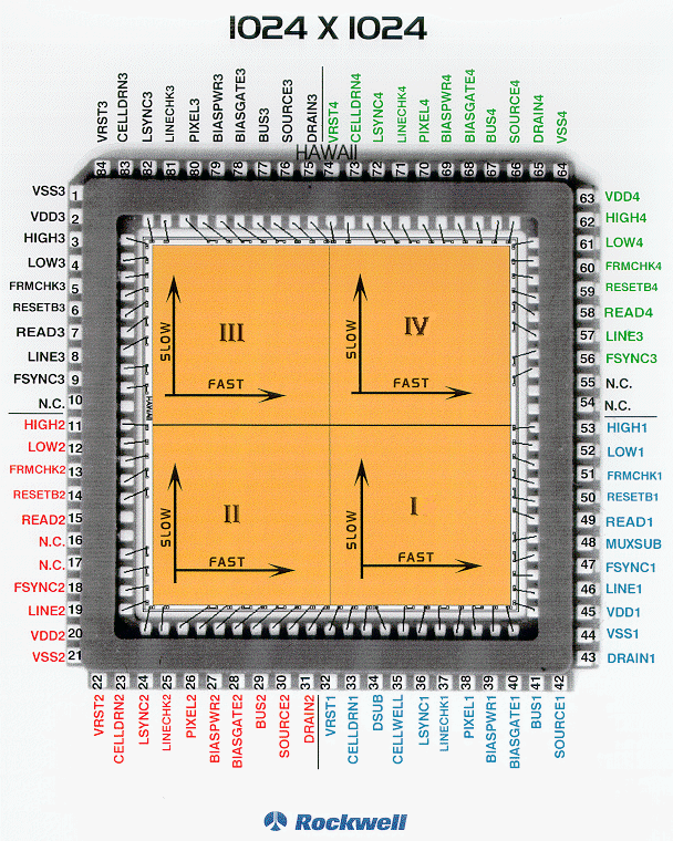 |
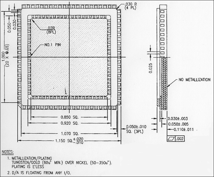
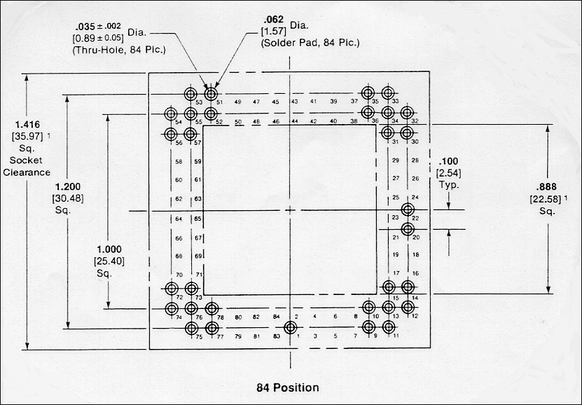
Pins |
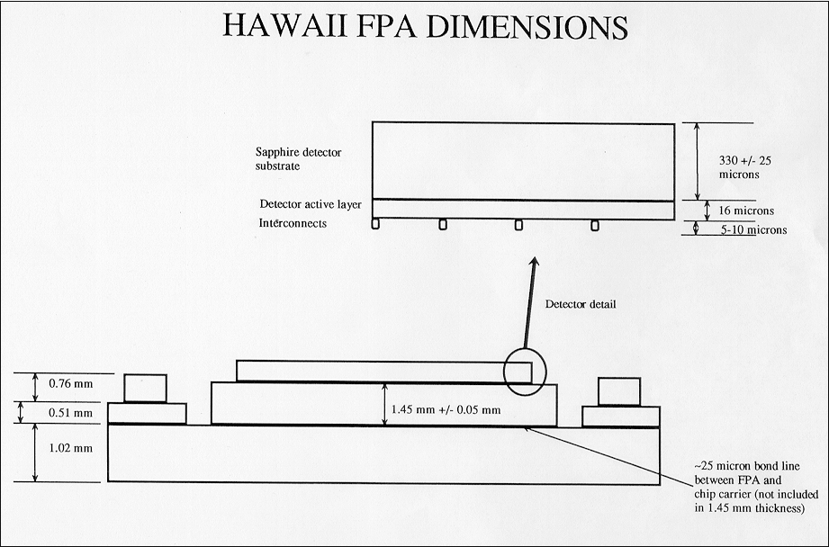  |
Array dimensions |
 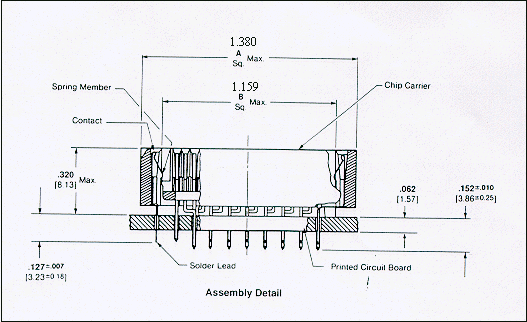 |
Socket |